Construction of a nanobalance with applications for microelectronics
A research group from the UAB Department of Electronic Engineering, the Institute of Microelectronics of Barcelona (CNM-IMB, CSIC), the UAB Research Park, and the EPFL Microsystems Laboratory of Lausanne, Switzerland, has created a nanobalance capable of detecting infimum amounts of matter. The sensor, a nanoscopic balance, is designed to measure fluxes of material in new lithography processes being developed to be used in the manufacturing of electronic microcircuits, and is capable of detecting fluxes measuring as low as 10 picometres per second. This will help build integrated electronic circuits which are even smaller than those existing now.
The sensor contains applications which measure the rhythm of material disposition in the lithographic processes used to manufacture the microcircuits which are the core part of any electronic device. The majority of circuits which make these devices work are manufactured by placing conductor material on an insulation tray and printing the circuit design. For smaller circuits this printing process requires a larger spatial resolution (being able to print very small dots) and a large precision and consistency in the quantity of conductor material deposited onto the tray. To achieve this precision at nanoscopic scale a shadow-masking lithography process is used in which the circuit shape is cut out to form a stencil which lets only particle fluxes of the different materials pass through the nanoscopic-sized apertures.
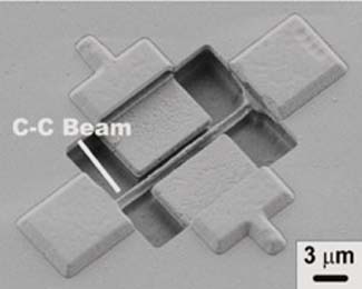
The nanoscale developed by scientists measures in real time the amount of mass deposited by registering the changes in resonance frequency of the nanoscopic lever. These changes in frequency are detected electrically thanks to the manufacturing of a nanolever in a CMOS oscillator, thus forming a totally integrated (NEMS-CMOS) and portable system. The system controls the stencil lithography disposition process with a resolution of only 100 nanometres and a precision in the measurement of material flux of only 10 picometres per second (higher than current quartz microbalances).
These types of nanobalances had been previously used to detect biomolecules and single cells and to detect chemical reactions or tiny masses (in the zeptogram-level range, 10-21 grams or 1000 times an atomic mass unit), but never before had they been used to monitor material fluxes flowing through nano- or micro-apertures in vacuum disposition systems. The research paves the way for a new generation of nanolithography systems which will permit the creation of integrated electronic circuits even smaller than those existing now.
The research was published on the cover of the nanotechnology journal Small and was carried out by Núria Barniol, Gabriel Abadal, Arantxa Uranga and Jaume Verd from the UAB Department of Electronic Engineering; Francesc Pérez Murano, Julien Arcamone and Marc Sansa from the Institute of Microelectronics of Barcelona (CNM-IMB, CSIC) and the CSIC centre at UAB's Research Park; and Marc van der Boogaard and Juergen Brugger from the EPFL Microsystems Laboratory of Lausanne, Switzerland.
References
Nanomechanical Mass Sensor for Spatially Resolved Ultrasensitive Monitoring of Deposition Rates in Stencil Lithography. Arcamone, J; Sansa, M; Verd, J, et al. SMALL, Volume: 5, Issue: 2 [176-180] (2009)