Silicon nanowires: better if longer
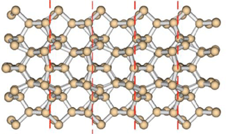
Silicon nanowires are silicon cylinders with a typical diameter of some tenths of nanometers. They are among the most promising one-dimensional systems for future applications in nanoelectronics and the possibility of using them as nanoscopic transistors has already been demonstrated. They have a good mechanical stability and, under certain conditions, they feature electron mobilities much higher than conventional silicon devices.
As in the case of traditional devices, if one wants to use nanowires as elements of some kind of (nano)electronic application it necessary to dope them, that is adding some impurities to modify in the desired way their electronic properties. These impurities, as any other defect, give rise to scattering of the electron current that has to be transmitted. Simplifying, it is like an ordered flux of point-like bodies that might run into some obstacles which, with a certain probability, can deviate their trajectory. It is clear than transmission will be much more efficient in absence of such obstacles.
In one-dimensional systems, like nanowires, impurity scattering is a limiting factor of growing importance of the performances. This happens because the defect cross-section can easily be of the same order of the wire's diameter. Hence, electrons can be backscattered, instead of being simply deviated.
For these reasons, the scattering properties of single dopants have been the object of many theoretic studies within the most accurate methods of quantum mechanics. In our work we show how it is possible to treat at the same level of precision realistic wires, that is longer and with different types of impurities at the same time. In this way, the simulation can provide magnitudes that can be more easily accessed experimentally, like mean free path -the mean path between scattering events- or the resistance as a function of length.
Not only the systems studied are more realistic, but they also present a much richer physics. For instance, when the wire is long enough it can end up in the Andreson localization regime. This is a fascinating phenomenon where the interference between successive scattering events drives the system into an operation region where Ohm’s law is violated and the resistance grows exponentially with the length, and not linearly as predicted by classical theory.
In this work, we have reported for the first time quantum mechanics simulations of distributions more or less complex of defects and not only of isolated impurities.
References
"Electronic transport through Si nanowires: Role of bulk and surface disorder - art. no. 245313". Markussen, T; Rurali, R; Brandbyge, M; Jauho, AP. PHYSICAL REVIEW B, 7424 (24): 5313-5313 DEC 2006.